ADC(Analog-to-Digital Converter)It is an electronic component that converts analog signals into digital signals. It usually has the following functions:
Sampling: Converting a continuous analog signal into a discrete time series;
Quantization: Convert the sampled signal amplitude into discrete digital values;
Encoding: Convert the quantized value into binary digital output.

TI's ADC chip schematic (data quoted from TI's official website)
JESD204 High-speed interface is a high-speed serial interface standard mainly used to connect data converters (such as ADCs and DACs) with logic devices (such as FPGAs).
JESD204A:Supports rates up to 3.125 Gbps;
JESD204B:Supports rates up to 12.5 Gbps;
JESD204C:Supports rates up to 32 Gbps;
Continued speed improvements enable the JESD204 standard to meet the growing demand for high-speed data conversion, especially in high-performance ADC and DAC applications.
The Challenges of Completely Testing an ADC
High-performance analog signal source, such as low phase noise, flat frequency response, good harmonic suppression, etc.
High-frequency testing: The sampling rate of ADC can reach several GHz or tens of GHz;
Digital interface testing: Integrity testing of the JESD204x high-speed digital output interface is also a challenge;
Dynamic range test: It is necessary to test the performance of ADC under large and small signals at the same time;
Complex testing methods and expertise also pose great challenges to complete ADC testing.

TI's ADC chip schematic (data quoted from TI's official website)
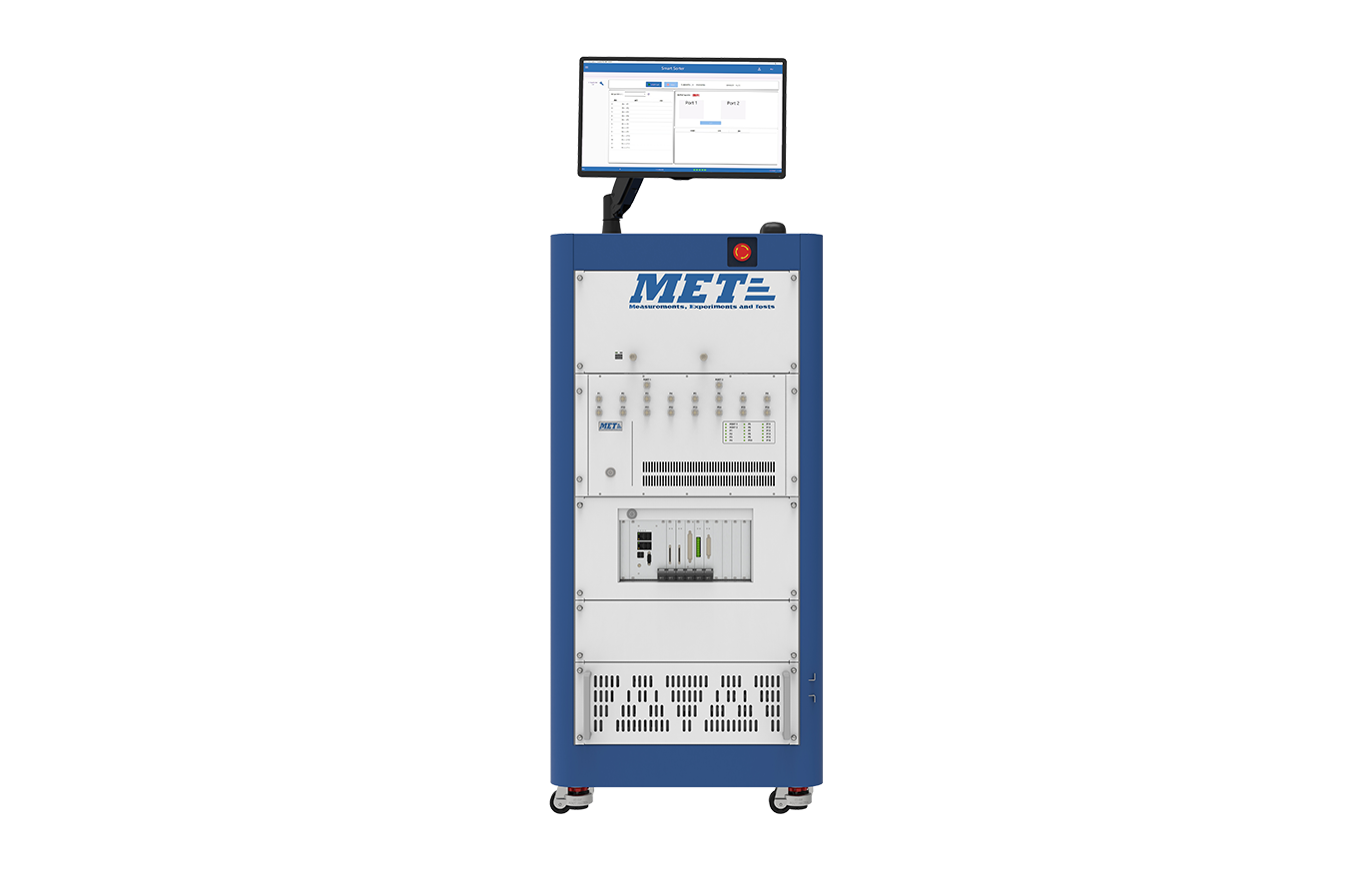
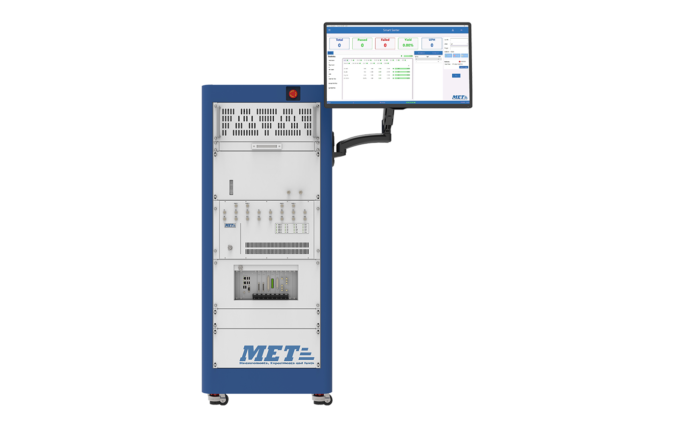
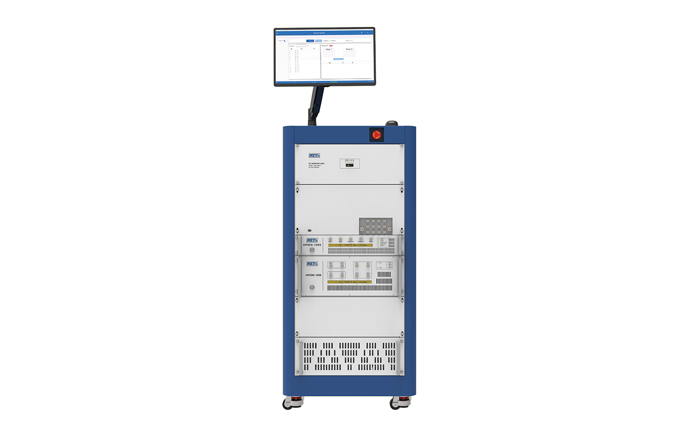
MET 的 AVATAR™-ADDA Testing Machine It is a turn-key solution designed for ADC/DAC/Transceiver chip testing. The system provides comprehensive ADC chip testing functions, including dynamic testing, static testing, logic testing, clock testing, and power testing.
The system uses MET's MVG-102B vector signal source, which supports dual-channel output in the frequency range of 10 MHz to 8 GHz. In response to the stringent test requirements of high-speed ADCs, especially the phase noise and frequency response flatness of the signal source, MET perfectly combines the MVG-102B vector signal source with the MCK-124A high-precision clock card to ensure the provision of high-precision, low-phase noise clock signals and external reference signals.

Vector signal source:MVG-102B

Frequency range … 10 M- 8GHz
Number of channels …… 2-CH
Instantaneous bandwidth … 600 MHz
Frequency step … 1 Hz
High-precision clock source:MCK-124A

Frequency range … 0.1~12.8 GHz
Output Power … -25~15dBm
Clock Channel … 4-CH
Reference Clock … 4-CH
Synchronous trigger … 4-CH
Phase Noise … 10GHz:-115dBc/Hz @10k
Jitter ……… 26 fs Typ.
MET High-speed ADC test solutions - dynamic test and static test
In addition to high-precision test hardware, MET has also developed ADLab-Suite high-speed ADC test software. The software is equipped with an intuitive wizard function that can effectively guide engineers to complete comprehensive test evaluations such as dynamic testing and static testing, significantly reducing the difficulty of operation.
Harmonic distortion (dBc or dBFS)
Total harmonic distortion (THD, dBc)
Full power bandwidth (MHz)
Analog input full scale (Vp-p)
Signal-to-noise ratio: SINAD, dB
Noise figure: NF, dB
Noise Floor (dBFS)
Effective number of bits (ENOB, Bits)
Spurious Free Dynamic Range (SFDR, dBc)
Signal-to-Noise Ratio: SNR
SNRFS,dBFS
Gain Error/Gain Matching
Offset Error/Gain Matching
Output high level/output low level
Differential nonlinearity error (DNL, LSB)
Integral nonlinearity error (INL, LSB)
Power Supply Rejection Ratio (PSRR, dB)

MET High-speed ADC test solution - JESD204B/C high-speed interface test
Currently, mainstream high-speed/high-resolution ADC devices generally adopt the JESD204B serial interface standard. This standard supports a transmission rate of up to 12.5 Gbps, effectively improving the data transmission bandwidth between ADC and logic devices (such as FPGA or ASIC).
JTesting ESD204B/C presents engineers with several challenges: How do you achieve the best design? How do you debug your system effectively? How do you ensure that your device meets specifications and operates properly during production line testing?
To address these challenges, MET developed a complete JESD204B/C test solution based on the SerDes PHY test recommendations in the OIF-CEI-0x specification released by the JEDEC standards organization and combined with actual needs.
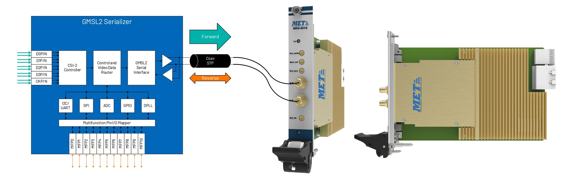
Using MET's MDO-401A high-speed oscilloscope, high-speed serial signals can be observed at a sampling rate of 40 GSa/s and 18 GHz bandwidth.


Bandwidth ……… 18 GHz
Resolution …… 8-bit
Sampling rate …… 40 GSa/s
Input Channels … 1-CH diff.
Input amplitude … 500 mVp-p
Record length … 500ms @40Gsa/s(20Gpts)
JESD204 Tx 一Conformity test items
|
JESD204 Tx Compliance Test |
|
Tx LOGIC OUTPUT |
Tx Jitter | ||
|
T_Baud |
Baud rate |
PJ |
Transmit uncorrelated bounded high probability jitter |
|
T_Vdiff |
Output differential voltage |
DJ |
Deterministic Jitter |
|
T_Vcm |
DC Common mode voltage |
DCD |
Transmit duty cycle distortion |
|
T_VcmAC |
Output AC common mode voltage |
TJ |
Total transmission jitter |
|
T_Rd |
Differential Impedance |
Eye Mask |
Transmission Eye Diagram Template |
|
T_Rdm |
Differential load impedance mismatch |
Others
|
Channel De-embedding |
|
T_tr, T_tf |
Output rise/fall time |
Clock frequency deviation measurement |
|
|
T_SDD22 |
Differential Output Return Loss |
Bit Error Rate Analysis |
|
|
T_SCC22 |
Common mode output return loss |
Power spectral density measurement |
|
Share:
News Center
2025-03-20News Center
2025-03-05News Center
2025-02-20


10th Floor, Building N4, Suzhou 2.5 Industrial Park, Dongchang Road, Suzhou Industrial Park, Suzhou City, Jiangsu Province
Copyright © Suzhou MET Technology Co., Ltd.- All Rights Reserved Web design